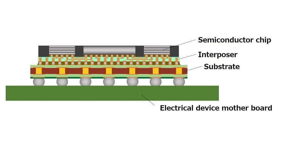
A standard CPU has three core parts. These are the substrate, the CPU die, and the IHS. The substrate is the PCB on which the rest of the CPU is placed. It has the CPU socket connector pins on its underside. The CPU die is the actual CPU. It’s precisely etched silicon that performs the processing. The CPU die also features the CPU cache tiers directly integrated to minimise communication times. The IHS is the Integrated Heat Spreader. It presses directly onto the CPU die and transmits the heat it produces to the CPU cooler. The IHS also offers protection against die cracking. The CPU die is fairly brittle, and the mounting pressure of the CPU cooler could crack it. The IHS neutralises this risk as it doesn’t transmit that pressure to the CPU die.
Multi-Chip Modules
The package substrate provides all the connectivity for the CPU die, routing the electrical signals from each of the used pins to the CPU die. Unfortunately, this doesn’t work quite as well when there are multiple dies on a single CPU. This may be because they’re using a standard chiplet architecture or because the design of the chip is more complex. For example, this would also apply if the CPU featured an FPGA or memory directly on the package. While MCM or Multi-Chip Module CPUs can work with just a substrate, as AMDs Ryzen CPUs show, an alternative, especially used in earlier chiplet designs was to use an interposer.
An interposer is simply an intermediary layer between the package substrate and the CPU die. The Interposer is made of silicon, which makes it fairly expensive, though not as expensive as more modern 3D die stacking techniques. The silicon interposer is typically configured to connect to the package substrate via a BGA, or Ball Grid Array. This is an array of small solder balls, which means that the interposer is physically held above the package substrate, compared to the CPU die which is directly fused to the substrate or interposer with electrical connectivity provided by copper pillars. The interposer then uses TSVs or Through Silicon Vias to pass the electrical signals through with no degradation. The silicon interposer also allows for die-to-die communication connectivity.

Benefits of using an interposer
An interposer offers two main benefits over placing the CPU die directly on the package substrate. Firstly, the silicon interposer has a much lower coefficient of thermal expansion. This means that smaller solder bumps can be used as the silicon can handle the increased thermal load. It also means that I/O connectivity can be significantly denser than when building directly on the substrate, allowing for higher bandwidths or better use of die space.
The second benefit is that silicon interposers can have much narrower traces etched into them than the substrate can. Allowing for denser more complex circuitry. Another advantage that may only affect some companies is that the silicon substrate can be etched with the use of legacy CPU etching hardware. If a company already has this hardware lying unused, it can be reused for this purpose. Modern small process nodes are not needed meaning that the hardware costs for the etching machinery is minimal, at least in comparison to modern fabrication nodes.
Conclusion
An interposer is an intermediary between the package substrate and the CPU die. It’s typically made of silicon. It offers good thermal stability for small-scale, high-density connections. This feature is particularly useful for chiplet-based CPUs.