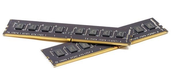
There are many different layers to addressing DRAM. DIMM is probably the most widely known, with a DIMM (Dual In-line Memory Module) being a stick of RAM. Ultimately memory is managed via a row and column address. There are plenty more layers in between, though. Memory is accessed over channels. Each channel is fully independent and can transmit data at the same time.
Note: While the channels are independent, they operate in lockstep and are synchronized. It’s essential to ensure that each populated channel operates at the same speed and has the exact timings. Ideally, all connected DIMMs should be identical and from one kit. Non-identical RAM can cause stability issues. If DIMMs of different speeds are connected, the fastest will be limited to the slowest speed.
On a DIMM, you have one or more ranks of DRAM chips. All chips in a rank are addressed at once and are essentially presented to the CPU as one larger DRAM chip. This works because data is spread across all the DRAM chips in a rank. For example, a channel has a width of 64 bits, and a DRAM chip has a width of 8 bits. 8 DRAM chips are needed to provide 64 bits of data to the data pins. The rank is essentially defined by the chip select, which acts as a bifurcator to the chips under its control. Each chip has several banks.
Banking on DRAM
In a single DRAM chip, there are multiple banks. The DDR4 spec allocates 4 bits to address banks, allowing for 16 banks per DRAM chip. Each bank is generally independent and can be in any phase of the access/refresh cycle. All banks have only one set of data pins. This configuration limits the DRAM chip to having only one bank transmitting or receiving data per clock cycle. It also allows for strong pipelining, which, under sufficient load, allows those data pins to be active on most, if not all, clock cycles rather than sitting idle while a new row opens.
Another key thing to know about banks is that they are entirely synchronized across a rank of DRAM chips. This synchronization is so complete that banks can be considered spanning all the DRAM chips in the rank.
A Worked Example
Let’s use an example; in this example, a read operation comes through to a rank to access bank 2, row 3, column 4. All DRAM chips in the rank will open row three, column four, in the second bank. Each will return 8 bits of data. The chip select that defines the rank will concatenate the data it receives into the 64-bit wide format of the channel and send it to the memory controller on the CPU.
Taking the example a little further, at the same time that bank 2 handles the read request, bank three can perform a refresh operation. Additionally, bank one can close its open row to prepare it to open a new one. Bank 7 can complete a read operation at the same time. However, it can’t send the data simultaneously as all banks share the same set of data pins. Bank 7 must wait for the data pins to be free to transmit its data.
Optimizations in the Banking System
By carefully pipelining the requests to all of the banks in a rank, the memory controller can ensure optimum usage of the data pins of both the DRAM chips and the channel in general. For example, suppose two read commands to two banks would overlap so that the second read operation would be left waiting for the data pins to be freed from the first. In that case, a refresh operation can be inserted into one or more other banks that aren’t otherwise in active use at that time.
Conclusion
Within a DRAM chip, there are several banks. Each bank can be independently operated, though they all share data pins. This means that access and refresh operations can be pipelined, but the actual data being written or read can only be received or sent by one bank at a time. Each bank seamlessly spreads over all DRAM chips in a rank, and these chips act in lockstep. Using banks, especially when access is optimized, helps to maximize the usage of the data pins when under a heavy enough load for that to be possible. Don’t forget to share your comments below.