Most computer users won’t particularly care about performance too much when they’re buying a computer. As long as it’s fast and cheap enough, that’s good enough. They’ll buy a computer with a current or previous generation CPU and look for the right amount of storage to the nearest half-terabyte.
Some may look for CPU speed, core count, or RAM capacity, but that tends to be it. If you’re a tech enthusiast, you may pay more attention to these things, so you know what you’re getting and if it’s really a good deal.
One of the ways to squeeze the most performance out of your computer is to get high-performance RAM. The significant flashy sales number is the clock speed of the RAM, such as DDR4-3200 or DDR5-6400. Technically that second number isn’t the clock speed. It’s the transfer rate. This is double the clock speed because DDR RAM is Double Data Rate. Still, the higher number sounds better on the marketing material.
That transfer rate is a measure of the bandwidth of the RAM, so higher numbers are better. Bandwidth, however, isn’t the only factor in RAM performance. Latency is just as important, if not more so.
Contents
What Is Latency?
Latency is a measure of the delay between a process being initiated and it actually happening. A simple example is the “ping” of your internet connection. If you’ve ever run a speed test, you’ll have seen your download speed and ping. The download speed is your internet bandwidth, and the ping is the latency between you making a request and the server receiving it. As many gamers will know, it doesn’t matter how fast your internet is. You won’t have a good experience if you’ve got high latency.
High-performance RAM will always advertise its speed. It will often advertise at least one specific measure of latency. The most common and important measure of latency is CAS Latency, sometimes shortened to CL. By looking a little deeper into the product specs, it’s generally possible to find the main four primary timings. These are tCL/tCAS (the CAS Latency), tRCD, tRP, & tRAS. These timings can occasionally be followed by a fifth number, a command rate, but that’s slightly different and generally unimportant.
The Basics of RAM Operation
Before we define those primary timings, it will be essential to understand the basics of how RAM actually functions. Data in RAM is stored in columns, and only one can be interacted with at any time. To be able to read from or write to a column, you first need to open the row in which that column is located. Only one row can be open at once. RAM can come with multiple banks. In this case, only one row can be available per bank. While only one column can be interacted with at once, having a second row open in a second bank allows the next read or write operation to be queued up efficiently.
It’s important to understand that timings are not absolute values. They are actually multiples of the RAM I/O clock as they are units of clock cycles. Again, RAM is Double the Data Rate, which is half the advertised speed. You need to do some math to determine the actual latency of specific timing. You can do 1/(advertised transfer rate in Ts/2) to get the length of a single clock cycle in seconds and then multiply that by the timing ratio you want to know the value of. Alternatively, suppose you want an easier time. In that case, you can do a 2000/advertised transfer rate in MTs to get the length of a single clock cycle in nanoseconds and multiply that by the timing ratio.
For example, if we’ve two sets of RAM, DDR4-3000 CL15 and DDR4-3200 CL16, we can do (2000/3000)*15 and (2000/3200)*16 to discover that the absolute CAS latency of both types of RAM is 10 nanoseconds.
Primary Timings
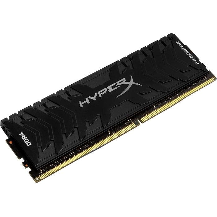
The primary timings of RAM are typically presented as a set of four numbers separated by dashes. Occasionally, these will be accompanied by either a “1T” or “2T” on end. For the following examples, we’ll use the primary timings from two entries in our recent article on the best gaming RAM in 2022: the G.Skill Trident Z Royal DDR4 3200 CL16-18-18-38 and the G.Skill Trident Z5 RGB DDR5 6400 CL32-39-39-102. For these examples, the primary timings are 16-18-18-38 and 32-39-39-102, respectively. The time for a single clock cycle is 0.625 nanoseconds and 0.3125 nanoseconds, respectively.
Note: All of these timings affect any operation, read or write, though, in the below examples, we’ll just refer to read operations to keep things simple.
CAS Latency
The first number in the primary timings is the CAS latency. This is typically the primary timing to improve if you’re trying to overclock the RAM. CAS latency can also be denoted at CL, tCAS, or tCL, with the latter two more likely to be found in the BIOS and other configuration utilities. CAS is short for Column Address Strobe. It isn’t technically a strobe anymore. But the command reads data from a column of an open row in what is known as a “page hit.”
tCL is a measure of how many cycles after a CAS instruction has been sent that the response will start to be returned over the I/O bus. So, for our DDR4 example, the CAS latency is 10 nanoseconds; for our DDR5 example, the CAS latency is also 10 nanoseconds.
RAS to CAS Delay
The second entry in the primary timings is the RAS to CAS delay. This will generally be denoted as tRCD and is a minimum value, not an exact value. If there are no rows open when a read instruction comes in, this is known as a “page miss.” A row must first be opened to access a column to read its data. RAS stands for Row Access Strobe. Like CAS, it’s not a strobe anymore with the name being a hangover, but it is the name of the command issued to open a row.
The RAS to CAS Delay is the minimum amount of clock cycles taken to open the row, assuming none is open. The time to be able to read data in that scenario is tRCD + tCL. Our DDR4 example has a tRCD of 18, which is 11.25 nanoseconds, while our DDR5 example has a tRCD of 39, which gives 12.1875 nanoseconds.
Row Precharge Time
The third primary timing is the Row Precharge Time, generally shortened to tRP. This value is essential when there’s another type of page miss. In this case, the right row is not open, but another row is. To open the right row, the other row must first be closed. The process of completing a row is called pre-charging. This involves writing the values to the row read from when it opened.
The Row Precharge Time is the minimum number of clock cycles required to complete the precharge process on an open row. The total amount of time to be able to read data from a cell, in this scenario, would be tRP + tRCD + tCL. As the values of tRP are the same as tRCD in both of our examples, it’s easy to see that they’d end up with the same values: 11.25 nanoseconds for the DDR4 tRP and 12.1875 nanoseconds for the DDR5 tRP.
Row Activate Time
The fourth primary timing is the Row Activate Time, generally shortened to tRAS. This is the minimum number of clock cycles between the command to open a row and the precharge command to close it again. It is the time needed to internally refresh the row. This is the only primary timing that overlaps with another, specifically tRCD. Values vary, but are typically roughly tRCD + tCL, though they can range up to around tRCD + (2* tCL).
Our DDR4 example has a tRAS of 38 cycles giving a total time of 23.75 nanoseconds. Our DDR5 example has an rRAS value of 102 cycles giving a total time of 31.875 nanoseconds.
Historically for synchronized DRAM, values have been very near tRCD + tCL, as seen in our example DDR4 timings. The tRCD + (2* tCL) scenario traditionally was used for asynchronous DRAM, as the memory controller needed to allow more than enough time for the operation to complete. Interestingly, DDR5 currently also uses the tRCD + (2* tCL) sum. It’s unclear if that’s caused by a change in the standard or if it’s a teething issue of early DDR5 products that will be tightened as the platform matures.
Interestingly, there is some evidence that it’s possible to boot with a tRAS lower than tRCD + tCL. Theoretically, this shouldn’t really work. It’s unclear if this is because this value, like most other timings, is a minimum and the memory controller chooses to use looser timings in practice. Or if the settings were only partially stable. Of the primary timings, this likely has the most minor effect on actual performance but may be worth adjusting if you’re after peak performance, especially with the high values seen in current DDR5.
Command Rate
The command rate is the number of cycles between a DRAM chip selected and a command executed on that chip. Many acronyms exist for this value, such as CR, CMD, CPC, and tCPD. The easiest way to tell is that the number value is typically followed by a “T.” Despite the T notation, this is still a measure in clock cycles.
Most RAM you find will run at 2T, though some may run at 1T. There will be a minimal difference as this is the difference of a single clock cycle, less than a nanosecond.
Secondary and Tertiary Timings
There are plenty of other secondary and tertiary timings that can be changed. However, doing so is highly complex. Even experienced memory overclockers can take a day or more to dial in stable settings. Some are easier to adjust than others and have more significant impacts. For example, tREFI and tRFC. These control how often the memory cells are refreshed and how long the refresh process takes. During the refresh process, the bank must otherwise sit idle. So having as large a gap between refreshes and as short a refresh period as possible means your RAM can function for more time.
Tuning these values shows a particular value when your RAM configuration has an insufficient number of banks. It’s critical to understand that getting these values wrong will cause large-scale memory corruption errors as the cells won’t be refreshed often enough. These settings are also susceptible to RAM temperature, as this directly affects how quickly the charge in a cell decays and thus how often it needs to be refreshed.
Memory Controller Ratio
Recent generations of CPUs can allow you to configure the memory controller ratio. This is typically known as Gear 1, 2, and 4. Gear 1 gets the memory controller to run at a 1:1 ratio with the memory. However, this results in excessive power draw above 3600MTs, affecting system stability. For some increase in latency, switching to Gear 2 runs the memory controller at a 1:2 ratio, at half the speed of the memory. This ultimately only offers any benefit from around 4400MTs and up. Gear 1 is better, but Gear 2 can provide stability at higher speeds.
While this is important for DDR4 RAM, DDR5 RAM currently always runs in Gear 2 as it starts out faster. While it’s presently unnecessary, as the technology is not mature enough to use, Gear 4 would operate the memory controller in a 1: ratio with the memory at one-quarter of the speed. Again, this is only necessary at high speeds. However, it is unclear exactly where this switchover would be as the hardware isn’t there yet.
Conclusions
RAM timings offer incredible configurability for your system RAM. However, they are also a deep rabbit hole if you get into full RAM overclocking. To help make it easier to get most of the benefits, the XMP standard allows memory manufacturers to specify their recommended timings outside of the JEDEC standards. This can offer extra performance in a nearly plug-and-play implementation.
In some cases, the XMP profile will get enabled by default. Still, often it will be necessary to select it manually in the BIOS. This automatically applies the higher vendor recommended speeds and tightens the timings to the vendor-tested settings. If you decide to configure your RAM timings, knowing what they are and what they do is essential.